Office Address: Sunmoon Science Park, 985 Xingzhong Road, High-Tech Zone, Bengbu, China Factory Address: Mohekou Industrial Park, Huaishang District, Bengbu, Anhui, China Contact: Ariel Young Phone: 0086-552-3827158 FAX: 0086-552-3822922 Mobile: 0086-15255290433 WebSite: www.siliconeoil.cn
www.siliconeoil.net
Email: sales@siliconeoil.net QQ:
|
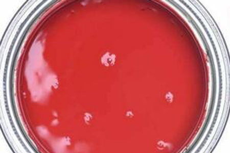
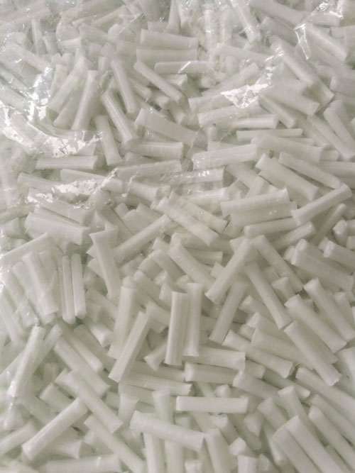
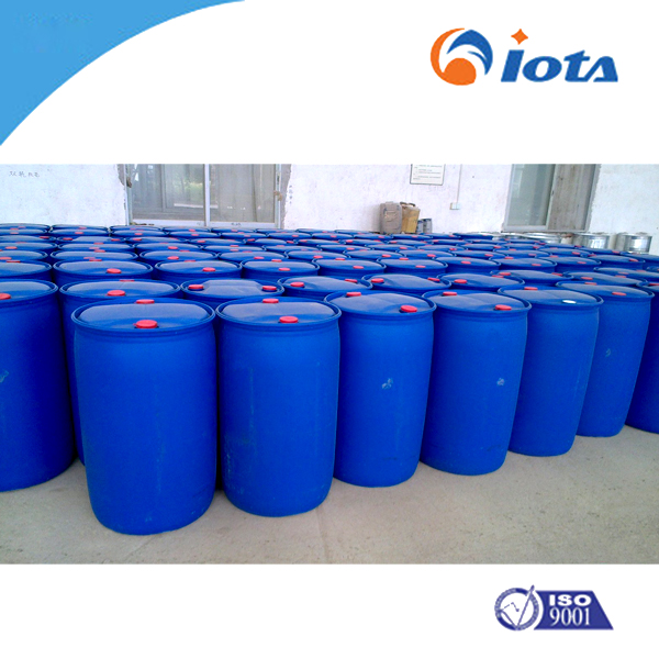
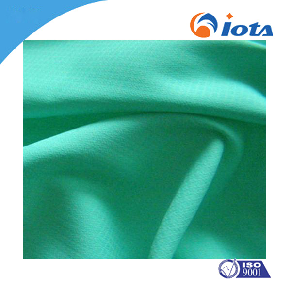
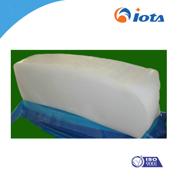
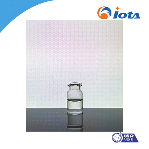
IOTA 6289 Methyl Silicone Resin for Concrete and Stone
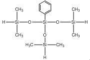
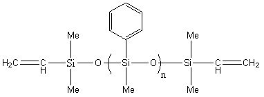
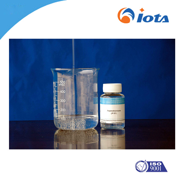
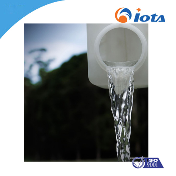
Polyethylsiloxane Fluids IOTA 2056 PES
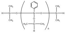
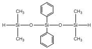
Ethyl Silicone Rubber IOTA 2056 HTV
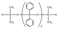
Ethyl Silicone Rubber IOTA 2056 GUM

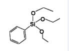
Single-terminated trimethoxyl-terminated silicone oil IOTA-2307
Mercapto modified silicone oil IOTA-280
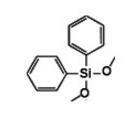
IOTA 5532 Methoxytriphenylsilane

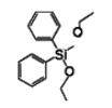
IOTA 5722 methoxy(methyl)diphenylsilane
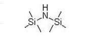
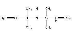
Tetramethyldisilazane IOTA 5205H

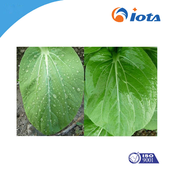
Super Hydrophobic Nano Ceramic Coating IOTA ST6
Fluoro Silicone Gum
Self-drying Silicone Resin IOTA 6605L
Self-drying Silicone Resin IOTA 6604
Methyl silicone resin IOTA 6080

IOTA 6608/6609 Pure Organic Silicone Resin Emulsion
IOTA 6607 Epoxy Organic Silicone Resin Emulsion

IOTA 6606 Acrylic Organic Silicone Resin Emulsion

IOTA 1501 Cyclopentasiloxane and Dimethiconol

IOTA 201-1 Octamethyltrisiloxane
Carbinol Silicone Oil IOTA 28300
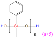
Phenol Terminated Silicone Oils
1,3-Bis(3-aminopropyl)-1,1,3,3-tetramethyldisiloxane IOTA2458

Hexamethylcyclotrisilazane IOTA-N202
Water-based silicone resin IOTA 6850S

Water-based silicone resin IOTA 6830S

Polyester modified silicone resin IOTA 6072A

Polyester modified silicone resin IOTA 6072-50D

Polyester modified silicone resin IOTA 6072-15
Polyester modified silicone resin IOTA 6038A
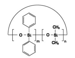
Methyl phenyl silicone resin IOTA 6156C

Methyl phenyl silicone resin IOTA 6153D

Methyl phenyl silicone resin IOTA 6056D

Methyl phenyl silicone resin IOTA 6056
Methyl phenyl silicone resin IOTA 6053G
Epoxy-modified silicone resin IOTA E60

Epoxy-modified silicone resin IOTA E30

Epoxy-modified silicone resin IOTA E25
Epoxy-modified silicone resin IOTA 6063-55
Alkyd modified silicone resin IOTA 6057

Acrylic polysiloxane resin IOTA BXS-90

Acrylic modified silicone resin IOTA 6146A

Acrylic modified silicone resin IOTA 6146
Acrylic modified silicone resin IOTA 6046
Organic Polysilazane IOTA 9283

Organic Polysilazane IOTA 9150K
IOTA 9028 Dichloro-bis(chloromethyl)silane
Non-foaming defoaming wetting agent IOTA 4100
Eco-friendly Solid Silicone Resin IOTA 6106
Eco-friendly Solid Silicone Resin IOTA 6105
Eco-friendly Solid Silicone Resin IOTA 6103
IOTA 3090A acrylic modified silicone resin

IOTA 1153D methyl phenyl silicone resin
IOTA 1146 acrylic modified silicone resin
IOTA 1127 polyester modified silicone resin

IOTA 1123 silicone resin intermediates

IOTA 1072A polyester modified silicone resin

IOTA 1063-55 epoxy modified silicone resin

Transparent super hydrophobic nano coating IOTA ST5
Carboxyl Silicone Oil IOTA 2520

Double-ended hydroxypropyl silicone oil IOTA 2030

Double-ended alcohol hydroxyl long-chain alkyl silicone oil IOTA 8865H

Double-ended alcohol hydroxy silicone oil IOTA 2110

Diol hydroxyl single-end long-chain alkyl silicone oil IOTA 8866

Diol hydroxyl single-end silicone oil IOTA 2176
Hydroxyl terminated methyl vinyl silicone oil IOTA 1203V
Acrylic Silicone Oil IOTA 2205

Single-ended hydroxypropyl silicone oil IOTA2050

Alcohol hydroxy single-ended long-chain alkyl silicone oil IOTA 8861

Single-ended alcohol hydroxyl silicone oil IOTA 2170
Side Chain Acrylate Modified Silicone Oil IOTA 170

Acrylic Silicone Oil IOTA 2220
Polycarbosilane adhesive IOTA H11500

Polycarbosilane adhesive IOTA H21500

Borosilazane adhesive IOTA H21400

Silazane Adhesive IOTA H21000

Silazane adhesive IOTA H31000
High temperature curing silicone sealant IOTA H1400

Modified cyanate ester adhesive IOTA RH3400C

Silicone resin modified cyanate ester Adhesive IOTA R3400

Fast curing high temperature resistant putty IOTA R31800F
High temperature resistant putty IOTA R31800

Silicone sealant IOTA R1400

Phenolic Modified Cyanate Adhesive IOTA R3600
Fasting curing silazane adhesive IOTA R3800F

Silazane ceramic precursor adhesive IOTA R31000

Silicone oxynitride adhesive IOTA R3800
High temperature resistant silicone adhesive IOTA R2400

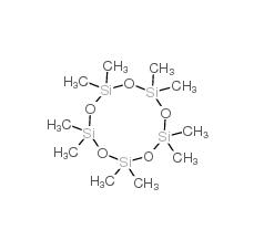
Hexamethylcyclotrisiloxane IOTA D3
high temperature resistant water-based nano ceramics coating IOTA ST4

Highest hardness Nano-coating in room temperature cured IOTA ST3
Waterborne nano high hardness self-cleaning coating IOTA ST2
Waterborne nano high hardness self-cleaning coating IOTA ST1
Low volatile silicone oil

Low viscosity hydroxyl fluoro silicone oil IOTA40F

Modified hydroxypropyl silicone oil (aqueous system)IOTA2040
Single-ended hydroxypropyl silicone oil IOTA2050
Bicomponent structured adhesive

IOTA 7000 (6000 Anti-fogging agent)
Epoxy double heads IOTA-010
Acrylate modified silicone oil IOTA 2032

Acrylate modified silicone oil IOTA 2031

IOTA 201-2 Dimethicone 2cst

Epoxy silicone oil chain extender IOTA 105-1000
Epoxy polyether silicone oil

IOTA 345 Cyclopentasiloxane and Cyclohexasiloxane

Drift control adjuvant IOTA-331
IOTA 9970

Silicon dioxides for coating
Hydrophobic series silica
IOTA FINE-SIL520A Silicon Dioxide

IOTA FINE Silicon dioxide

IOTA 96212 Silicone Elastomer Gel

IOTA 96211 Silicone Elastomer Gel
IOTA 96082 Silicone Resin Elastomer Suspension
IOTA 96061 Silicone Elastomer Powder
IOTA 96004 Silicone Resin Elastomer Gel

IOTA 9609 Silicone Elastomer Gel

IOTA 9608 Silicone Elastomer Suspension

IOTA 9607 Silicone Elastomer Gel
IOTA 9606 Silicone Elastomer Powder
IOTA 9600D Silicone Elastomer Gel

IOTA 9600B Silicone Elastomer Gel

IOTA 9600 Silicone Elastomer Gel

Organic polyborosilazane (Potteryable precursor polymer) IOTA 9120
Nano silica dispersion IOTA 100F1, IOTA 100F2
Hydrophobic Silica IOTA 90-02

Hydrophobic Nanometer Silica IOTA 90-01
Hydrophilic type nano-silica IOTA 100
Anti-graffiti silicone resin IOTA-TC1
IOTA 5803 Methyltriphenylsilane

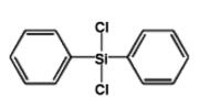
Methyl phenyl dichlorosilane IOTA5804
Organic polysilazane IOTA 9108

Organic polysilazane IOTA 9118
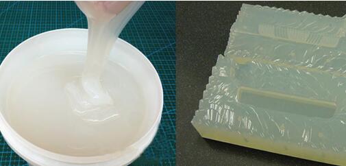
High transparency mold making silicone rubber
Food grade silicone rubber for mold making
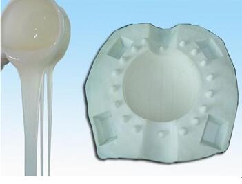
Condensation type mold silicone rubber
High refraction index phenyl silicone packing gel IOTA 34255

High temperature lubricating oil IOTA-255B

High temperature resistant silicone oil IOTA-255A
Organic silicon industrial cleaning agent IOTA2018

Sealed silicone grease IOTA 2014

Thermal Grease IOTA 2013

Lubricating silicone grease IOTA2012

OctaMethyltetrasiloxane IOTA2101

Methyl-bis(trimethylsilyloxy)silicon IOTA2100

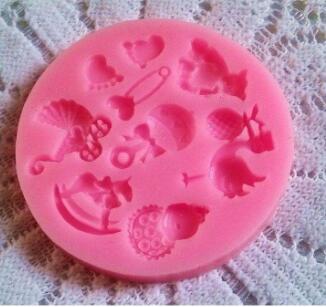
Silicone products multi holes cake mold IOTA 41007
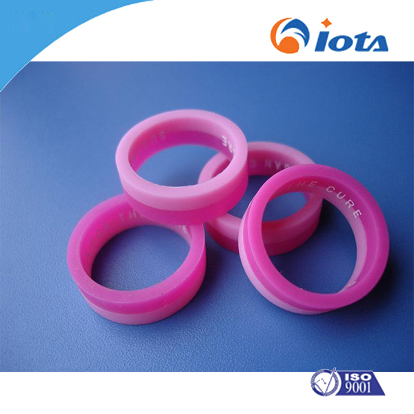
silicone rubber material for Flame retardant high temperature resistant IOTA 26E9-40,50,60
Silicone rubber material for swimming class equipment with IOTA351-20, 30, 40, 856-20, 221-20
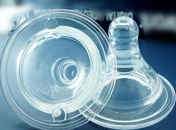
Silicone rubber material for Medical apparatus and instruments IOTA5971-60*, 70* ,80*,IOTA971-60* ,60K
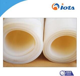
Liquid silicone rubber material IOTA-6120 15, 20, 20-H
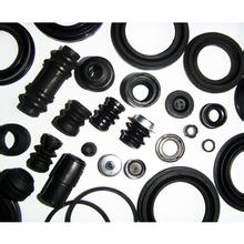
Silicone rubber material for auto parts IOTA 231-20*
Silicone rubber material for wire, tubular product IOTA4366-30, 40, 50, 60, 70, 80

Silicone rubber material for wearable digital electrical accessories IOTA 151-30A, 40A, 50A, 60A, 70A, 80A
Silicone rubber material for home appliance accessories and miscellaneous pieces IOTA151-10, 20, 30, 40, 50, 60, 70, 80, 90
Silicone rubber material for industrial products IOTA9241-20*,30*,40*,50*,60*
Silicone rubber material for electrical power, communication IOTA141-40*, 50*, 60*

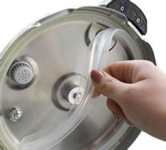
Silicone rubber material for Kitchen utensils and appliances industry class IOTA151-10, 20, 30, 40, 50, 60, 70, 80, 90
Silicone rubber material for office automation IOTA151-30, 40, 50

IOTA GF998 Fire Resistant Silicone Weatherproofing Sealant

IOTA 1098 High Performance Silicone Weatherproofing Sealant

IOTA GF999 Fire Resistant Silicone Structural Glazing Sealant

IOTA 1092 High Performance Silicone Structural Glazing Sealant

IOTA 998 Silicone Weatherproofing Sealant

IOTA 997 Silicone Sealant For Stone Applications

IOTA 995 Silicone Sealant For Total Vision System

IOTA 992 Silicone Structural Glazing Sealant

IOTA DJ310 Hollow glass hot melt butyl rubber
IOTA 119 Fire Resistance Silicone Sealant

IOTA 997 Silicone Sealant For Stone Applications

IOTA 993 Silicone Sealant for Skylight

IOTA 887 Dry hanging stone elastic rubber

IOTA 886 Silicone Structural Insulating Glass Sealant

IOTA 882 Silicone Insulating Glass Sealant
IOTA GZ series Thermal conductive silicone
IOTA 3400 Silicone heat conductive gasket

IOTA 3300 Silicone heat conductive gasket

IOTA 3100 Silicone heat conductive gasket

IOTA800FG Thermal insulator sheet

Cationic hydroxy silicone oil emulsion IOTA-2051

Anionic hydroxy silicone oil emulsion IOTA-2052

Epoxy silicone oil emulsion IOTA-1051

Hydrogen silicone emulsion IOTA 2021
Precipitated Silica IOTA9002
Silicone wax
IOTA SA408FG Thermally conductive double-sided adhesive tape
IOTA 4815W single component silicone sealant

IOTA 4815Z single component silicone sealant

IOTA 4815C One component silicone sealant

IOTA DJ330 Hot melt butyl
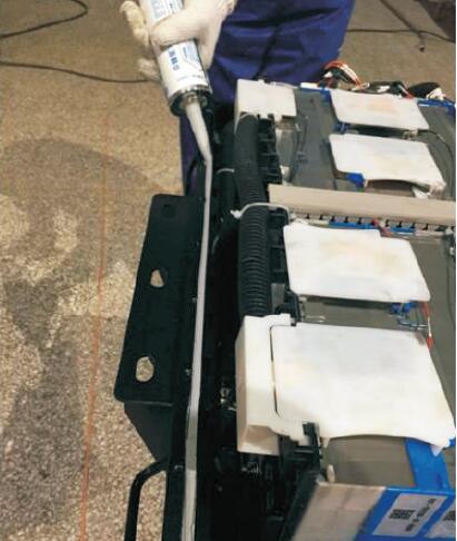
IOTA 4926 Silicone sealant for new energy automotive safety power

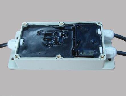
IOTA 4808 Silicone Electronic Potting Sealant

IOTA 888A Silicone Sealant for Solar Modules
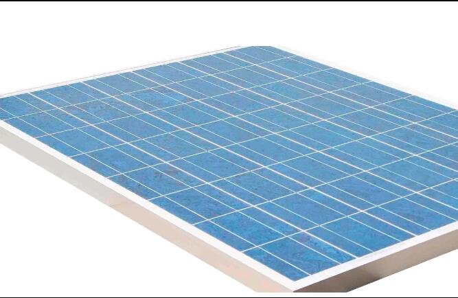
IOTA 855 Silicone Sealant for Solar Modules
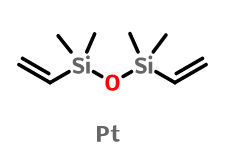
Platinum(0)-1,3-divinyl-1,1,3,3-tetramethyldisiloxane (the platinum catalyst) IOTA-8100

High temperature resistant silicone emulsion IOTA 240
Hexamethyldisilane IOTA-5002
Pentamethylphenyl dihydrotrisiloxane IOTA-2238
Vinyl terminated T-type phenylpolysiloxane IOTA-253
Epoxy-terminated phenyltrisiloxane IOTA-279
Epoxy-terminated phenyltrisiloxane IOTA-278
High elastic foam silicone strip IOTA-4801
High elastic silicone foam sheet IOTA-4800
Phenyl silicone oil emulsion IOTA PEMUL 255

New type of silicone chain extension agent IOTA-4001

High refractive index plasticizer IOTA-9006
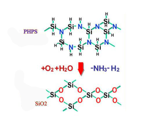
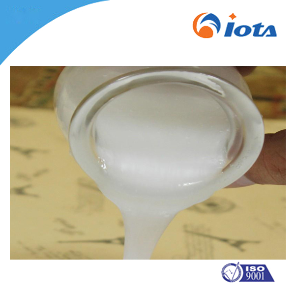
Perhydropolysilazane IOTA-PHPS

Heat Curable Coating Resin IOTA-OPSZ-1800
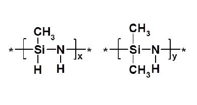
Organopolysilazane IOTA-OPSZ-9150

LED GEL refractive index regulator IOTA-9005
High refractive index silicone oil IOTA-259A
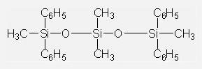
Dimethyltetraphenylsiloxane IOTA 259
Tetraphenyldimethyldisiloxane
Pentachlorophenyl trichlorosilane
Tetrachlorophenyl trichlorosilane
AB Liquid Silicone rubber foam IOTA-663
IOTA 201-1.5 Dimethicone 1.5cst

Silicone waterproof coating IOTA-301
Copolymer resin series mold materials for foam lost casting IOTA-STMMA
Long Glass Fiber Reinforced Polyamide IOTA-LFT-PA
Long Glass Fiber Reinforced Polypropylene IOTA-LFT-PP

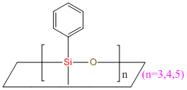
Methylphenyl silicone resin IOTA-B202

Phenyl silicone resin IOTA-B201

Epoxy-modified silicone resin IOTA H-60

Epoxy-modified silicone resin IOTA-H-30
Polyester modified silicon resin IOTA-1062G
Modified silicone resin IOTA-1057

Pure silicone resin IOTA-1056D

Pure silicone resin IOTA-1056
Pure silicone resin IOTA-1053G

Polyester modified silicone resin IOTA-1046

Polyester modified silicone resin IOTA-1038A
Phenyltriethoxysilane IOTA-531
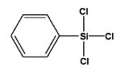
Phenyltrichlorosilane IOTA-525
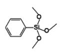
Phenyltrimethoxysilane IOTA-530
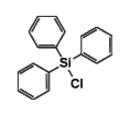
Triphenylchlorosilane IOTA-529
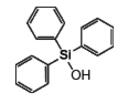
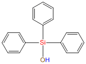
Triphenylsilanol IOTA-528
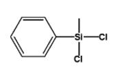
Methylphenyldichlorosilane IOTA-527
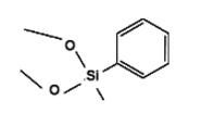
Methylphenyldimethoxysilane IOTA-526
Dimethyl Diphenyl Cyclics IOTA-524
Diphenyldiethoxysilane IOTA-523
Diphenyldichlorosilane IOTA-522
Diphenyldimethoxysilane IOTA-521

Silicones for Technical Fabrics and Leathers IOTA-TCS-7001

PHENYL SILICONEGUM(HTV)IOTA- 34
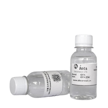
Diphenyl tetrasiloxane IOTA 234
Phenyl-tris(dimethylsiloxy)silane IOTA 235
Phenylsilsesquioxanes hydrogen-terminated IOTA 233
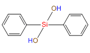
Dihydroxydiphenylsilane(DPSD) IOTA R05
Cyclophenylmethicone IOTA R21

High security hydroxyl silicone oil for fumed silica IOTA 1203D

Linear hydroxyl silicone oil IOTA 1203M

Hydroxyl blocking methyl vinyl silicone oil IOTA 1203V
Methoxy blocking polymethyl silicone oil IOTA 1204A

Ethoxy blocking polymethyl silicone oil IOTA 1204B
Methyl phenyl methoxy silicone oil IOTA 1204C

DIMETHICONE IOTA DM 10

DIMETHICONE IOTA DM50 - DM1000

DIMETHICONE IOTA DM5000 – DM60000
Cyclopentasiloxane IOTA CM5 A2

Low Viscosity Silicone Oils IOTA PDMS 47V3 - 47V10

Middle Viscosity Silicone Oils IOTA PDMS 47V50 - 47V1000
High Viscosity Silicone Oils IOTA PDMS 47V5000 - 47V500000
Personal care silicone oil IOTA 29161
Triphenylsilanol IOTA R06
MePhOH-group silicone oil IOTA R32
Hexamethyldisilazane(HMDS) IOTA 011
Vinyl silazane IOTA 51001
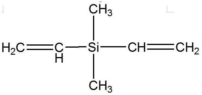
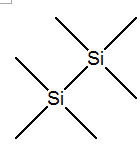
Dimethyldivinylsilane IOTA-501

Dual-head vinyl silicone oil IOTA VM-19

Multi-vinyl silicone oil IOTA VM-26

Cyclopentasiloxane dimethiconol IOTA 1021 IOTA 1022
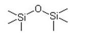
Hexamethyldisiloxane IOTA 005
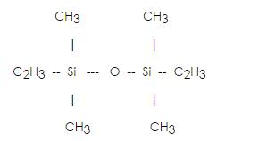
Divinyltetramethyldisiloxane(Vinyl double heads) IOTA 1002

Methylphenyldiethoxysilane IOTA-826

Diethoxydiphenylsilane IOTA-814

Diphenyldimethoxysilane IOTA-813

Phenyltriethoxysilane IOTA-802
Phenyltrimethoxysilane IOTA-801

Trimethoxysilylpropanethiol IOTA-590

3-Mercaptopropyltriethoxysilane IOTA-580

3-Ureidopropyltriethoxysilane IOTA-1160

γ-Ureidopropyltrimethoxysilane IOTA-1524
Anilino methyl triethoxysilane IOTA-42
Bis(trimethoxysilylpropyl)amine IOTA-1170

3-(2-Aminoethylamino)propyl-diethoxymethylsilane IOTA-5702

N-(2-aminoethyl)-3-aminopropylmethyl-dimethoxysilane IOTA-602

N (2-aminoethyl) -3-aminopropyltriethoxy-silane IOTA-910

N (2-aminoethyl)-3-aminopropyltrimethoxy-silane IOTA-792

3-(Diethoxymethylsilyl)propyl methacrylate IOTA-671

3-(Triethoxysilyl)propyl methacrylate IOTA-670
3-Methacryloxypropylmethyldimethoxy silane IOTA-571

3-methacryloxypropyltrimethoxysilane IOTA-570

3-Glycidoxypropyltrimethoxysilane IOTA-560

Vinyl tris(2-methoxyethoxy) silane IOTA-172

Dimethicone and Dimethiconol IOTA1403

Cyclopentasiloxane (and) Cyclotetrasiloxane (and) Dimethiconol IOTA1401

Methyl phenyl vinyl silicone rubber IOTA 120

Hexamethyldisilazane(HMDS) IOTA 011

Dimethyl Vinyl Ethoxy Silane (Vinyl single end ) IOTA-DVES

Trimethylchlorosilane M3
Powder Agricultural Silicone synergist IOTA2001

High temperature resistant release agent emulsion IOTA-257-60
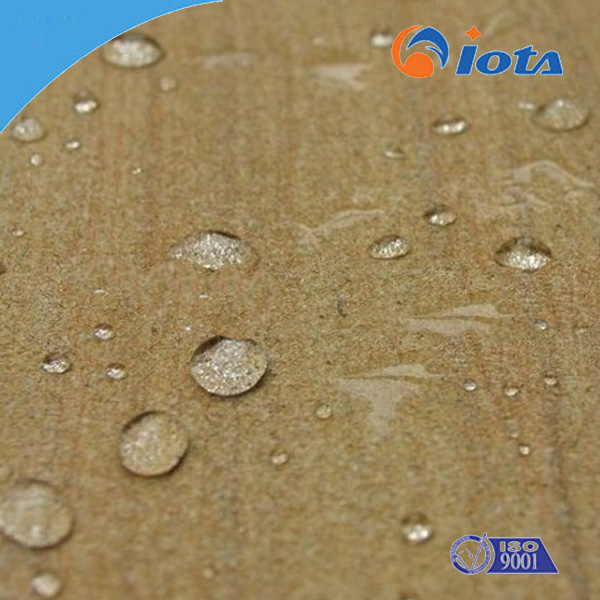
IOTA BP9500 Building protective waterproofing agent
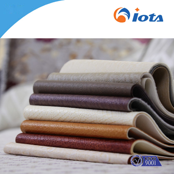
Silicones for Technical Fabrics and Leathers IOTA 7001

IOTA 1647V75 Organo Functional

Leather processing waterproofing agent IOTA 1669

IOTA 70827A EMULSION CATALYST

Water Repellent IOTA EMUL 269

Water Repellent Treatment IOTA WR 68

Building Protection Water repellent additive IOTA BP 9705

Water based coating release agent IOTA MR5900

Solventless methyl silicone resin release agent IOTA RES 9515

Release agent IOTA 2206

Universal defoamer agent IOTA C585

High-performance silicone-based organic silicon compound IOTA C583
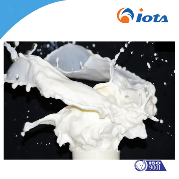
High-performance silicone-based organic silicon compound IOTA C581
Black liquor defoamer IOTA C563

Silicone defoamers IOTA C545
Low refractive LED Encapsulants
Methyl vinyl MQ silicone resin IOTA-AM

Methyl hydrogen cross-linking agent IOTA-AF
Octaphenyl cyclotetrasiloxane IOTA-AKT

Smooth and standing silicone oil for cotton IOTA 805

Super soft hydrophilic block silicone oil for cotton IOTA J50A
Super soft smooth hydrophilic block silicone oil for cotton IOTA N30
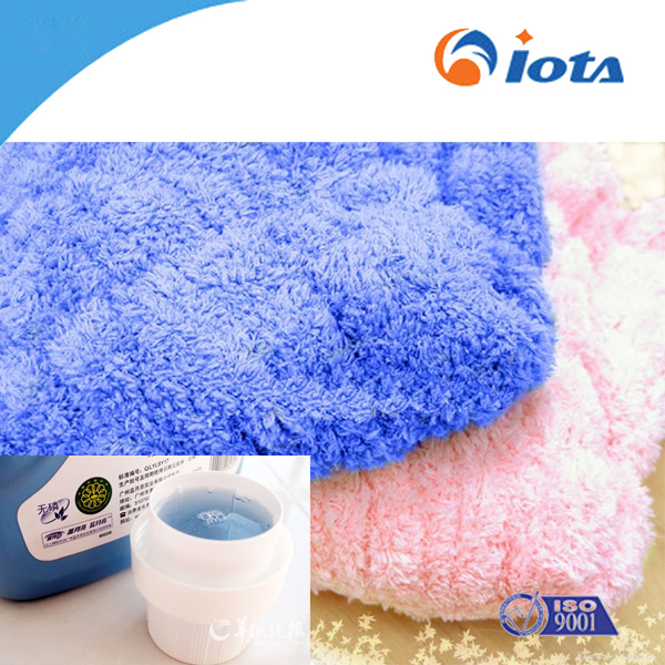
Smooth and soft silicone oil for cotton IOTA 817

vinyl ketone group, the crosslinking agent IOTA-91

Phenyltris methylethylketoximio silane IOTA-36

Methyltris(methylethylketoxime)silaneblend IOTA-32

Methyltrimethylethylketoximesilaneblend IOTA-31

Tetraethxoysilane-40 IOTA-130(Si40)

Ethyl silicate / Four oxygen radical IOTA-130(Si28)
Tetramethoxysilane (methyl orthosilicate) IOTA-5101
Methyltriethoxysilane IOTA-150

1,2-bis trimethoxysilyl ethane IOTA-26

Poly methyl triethoxysilane IOTA-23
Methylethyl triacetoxy silane IOTA-18
Methylpropyltriacetoxysilane IOTA-17

Propyl triacetoxy Silane IOTA-16

Ethyl triacetoxy silane IOTA-15

Modified methyltriacetoxysilane IOTA-13

Modified Methyltriacetoxysilane IOTA-12

Di-t-butoxydiacetoxysilane IOTA-11

Methyltriacetoxysilane IOTA-10

Mercaptopropyltriethoxysilane IOTA580

Vinyltris methoxyethoxysilane IOTA 172

Vinyltriethoxvsilane IOTA 151

aminopropylmethyldiethoxysilane IOTA 902

aminopropylmethyldimethoxysilane

Aminopropyltriethoxysilane IOTA 550

Trimethoxysilane IOTA 160
Construction sealant Oxime
Construction sealant Acetic

High transparent liquid silicone rubber LSR IOTA 6300
High tear strength and high temperature vulcanized silicone rubber IOTA HD
Safety cable silicone rubber MF IOTA 8465

High damping coefficient and resistance to low temperature IOTA MM 771 Series
High temperature stability silicone rubber IOTA THT

Outstanding high mechanical properties silicone rubber IOTA HP Series
High rebound and low compression set silicone rubber IOTA HCR 2900 Series

Good mechanical properties general silicone rubber IOTA HCR 1900 Series

Economic general silcone rubber IOTA HCR 1600 Series

Process ability silicone rubber IOTA HCR 9100 Series

High rebound silicone rubber IOTA HCR 900 Series

High tear stength and high transparent silicone rubber IOTA HCR 300 Series
High transparent extrusion silicone rubber IOTA HCR 100 Series
IOTA 795 Methyl vinyl silicone rubber
IOTA 759 Methyl vinyl silicone rubber
IOTA 755 Methyl vinyl silicone rubber
IOTA 753 Methyl vinyl silicone rubber
IOTA 751Methyl vinyl silicone rubber

IOTA107 V150000-V550000 High viscosity linear hydroxyl-terminated polydimethylsiloxane
IOTA107 V5000-V80000 low viscosity linear hydroxyl-terminated polydimethylsiloxane

IOTA 107 V500-V3000 low viscosity linear hydroxyl-terminated polydimethylsiloxane
IOTA1021Cyclopentasiloxane IOTA 1022Dimethiconol
Low compression set silicone rubber IOTA HCR 200 series
IOTA D5 Cyclopentasiloxane
RTV Methyl silicone rubber

Methyltrichlorosilane
Methyldichlorosilane

Dimethyl siloxane cyclics mixture

Dimethylchlorosilane
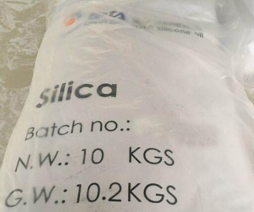
Silica

Octamethylcy-clotetrasiloxane

High efficient automobile detergent IOTA111
High efficient laundry detergent IOTA110
Smooth softener IOTA 17530
Polyester fluffy agent IOTA 17540
Divinyl-terminated methyl phenyl siloxane IOTA252

Methyl MQ silicone resin IOTA1200
Methyl MQ silicone resin IOTA7080 (powder)

Mica adhesive IOTA-500

Wetting agent IOTA245

High temperature mold release agent
High temperature resistant silicone oil

water soluble silicone oil IOTA-1291
Polydiethylsiloxane (lubricant oil or instrument oil )

Dicyclopentyldimethoxysilane (D-Donor)

Cyclohexyl methyl dimethoxysilane (CMMS)

Tetra methylethylketoxime silane TOS

Methyltris methylethylketoxime silane (MOS)
Tetrapropoxysilane IOTA-933

Mercaptopropyltrimethoxysilane IOTA-80
Methacryloylpropyltrimethoxysilane IOTA-70

Epoxypropoxypropyl trimethoxysilane IOTA-60
Methyl phenyldimethoxysilane MPDMS
Diphenyldimethoxysilane DDS
Aminoethyl aminopropyl trimethoxysilane DAMO

Aminopropyltriethoxysilane AMEO

Vinyltrismethylethylketoximesilane VOS

Tetravinyltetramethylcyclotetrasiloxane V4

Vinyltrimethoxysilane VTMO
High performance lubricant release agent
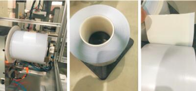
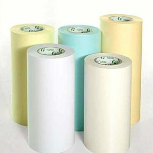
Glassine silicone paper
CCK Silicone Paper
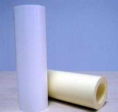
CCK Release Paper
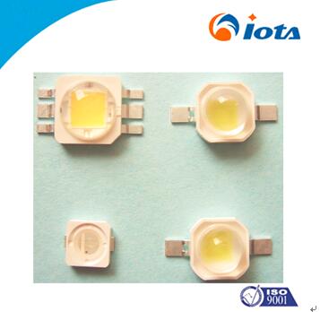
High refractive index LED package silicone gel IOTA4011
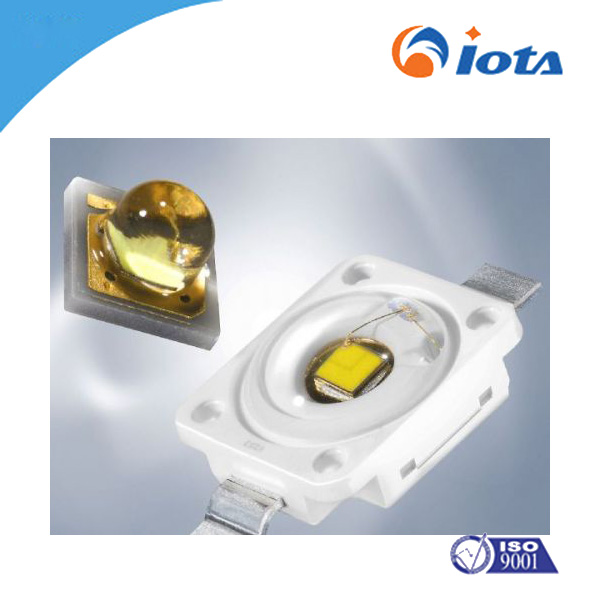
High refractive index LED package silicone gel IOTA4022
LED package Silicone gel IOTA3011
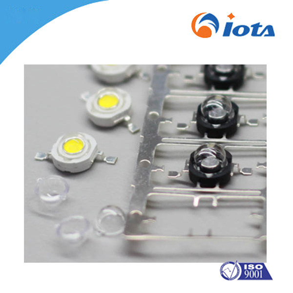
LED package silicone gel thickener IOTA204

Phenyl methyl hydrogen silicone resin IOTA207
Methyl phenyl vinyl silicone resin IOTA208

Phenyl-trisilane

Hexamethyldisilazane

Hexamethyldisiloxane IOTA 005
Triphenylchloromethane
7-methyl-3-siloxane
epoxy silicone oil

pigment printing thickener
polyester printing thickener
Chemical Fiber smoothing agent

Polyester smooth agent

Hydrogen termniated silicone oil

Tetramethyldisiloxane IOTA 606

Methyl Low Hydrogen silicone oil

Methyl High Hydrogen silicone oil
Dimethyl chlorosilane
TETRAMETHYLCYCLOTETRASILOXANE
Tetramethyl diphenyl trisiloxane

Hydride terminated polyphenylsiloxane
Hydride terminated polydiphenylsiloxane
Hydrogen MQ resin

Vinyl silicone oil

Side chain type vinyl silicone oil

Tetramethyl diphenyl tetrasiloxane
Methyl silicone oil emulsion

Long chain alkyl silicone oil IOTA 2320
Divinyltetramethyldisiloxane(Vinyl double heads) IOTA 1002

Methyl phenyl resin IOTA-955

Methyl silicone resin IOTA 6070
Amino silicone oil IOTA 100
Amino silicone oil emulsions

Block amino silicone oils

Low viscosity silicone oils and Volatile silicone oils

Dimethicone methyl silicone oils IOTA 201

Hydroxyl silicone oils
Thread silicone oils IOTA205
High grade release papers
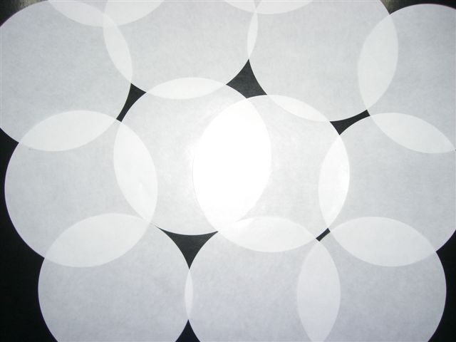
Glassine paper
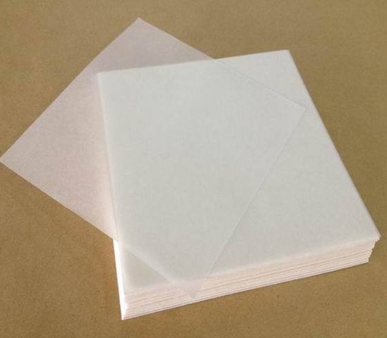
Food grade greaseproof papers
Food grade silicone papers

Leveling Agents Iota3000

Agricultural silicone surfactants IOTA-2000
Vacuum Diffusion Pump Oils IOTA705
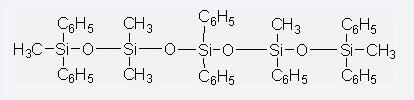
Phenyl Methyl Silicone Oils IOTA250-30
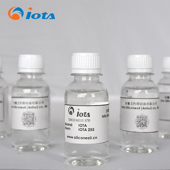
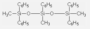
Phenyl Methyl Silicone Oils IOTA255
Phenyl Methyl silicone oil IOTA 556 (Phenyl Trimethicone, Cosmetic grade fluid)

Vacuum Diffusion Pump Oils IOTA702
Vacuum Diffusion Pump Oils IOTA704
皖ICP备14007495号
Copyright © 2000-2026 Iota Silicone Oil (Anhui) Co., Ltd, All Rights Reserved


